
Semiconductors
Packaging, developement and production control
- Perform structural and failure analysis for process development, yield improvement and construction analysis of advanced semiconductor packages, including 2.5/3D and fan-out packages
- Analyze printed circuit boards for reverse engineering and hardware security
- Non-destructively image across length scales from module to package to interconnect for submicron-resolution characterization of defects at speeds that can complement physical cross-sectioning
- Enable better understanding of defect locations and distributions by viewing unlimited virtual cross-section and plan-view images from all desired angles
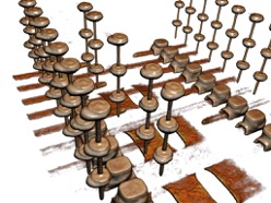
DRAM package interconnect within a 10 mm x 7 mm x 1 mm package containing a 4-die stack. Solder extrusion is easily visualized in 3 dimensions, 0.8 µm/voxel (Source: https://www.zeiss.com/microscopy/int/products/x-ray-microscopy/zeiss-xradia-610-and-620-versa.html)
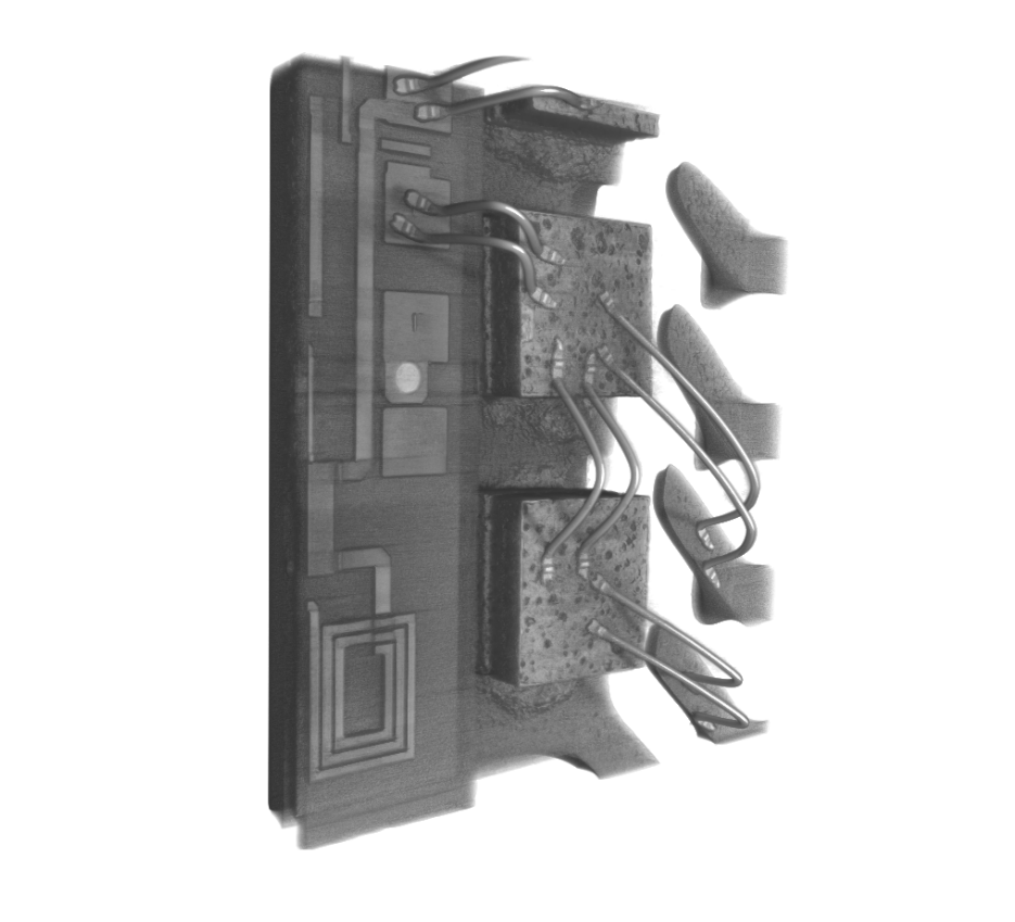 Detailed Image of Interconnect’s solders easily visualized in 3 dimensions. Pixel Size 1.76 µm. (Source: F. Cognigni, Xradia Versa 610 – CNIS – Sapienza University of Rome and Carl Zeiss SpA.
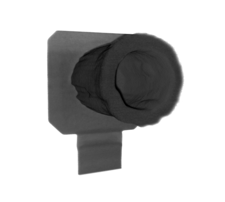
3D rendering of a Via Hole from an Integrated Circuit. Pixel Size 0.20 µm Xradia Versa 610 – CNIS – Sapienza University of Rome
Via Hole